Symposium on Future Electronics

This presentation will provide an overview of GE’s vertically integrated activities from SiC devices and modules to converters for MW-scale industrial applications. GE has developed a new generation of high performance SiC MOSFETs with voltage ratings from 1.2 to 3.3kV and current ratings up to 100A per chip. Significant progress has been made toward the goal of demonstrating the MOSFET reliability comparable to mature silicon IGBTs. Extensive stress testing has also mapped out the device’s safe operating area, including avalanche capability, short circuit ruggedness, body diode surge and stability, and terrestrial cosmic radiation hardness.

In addition, a portfolio of low inductance half-bridge modules for fast-switching SiC MOSFETs will be described. By taking advantage of the MOSFET’s body diode, the modules do not require anti-parallel diodes, saving cost and freeing up floor-space for additional MOSFETs. When compared to silicon modules with the same mechanical footprint and voltage ratings (e.g. 1.7kV), the SiC modules deliver twice as much current (500Arms), even when operating at three times higher switching frequency (7.5kHz vs. 2.5kHz).

For more than half a century, the growth of the semiconductor industry’s footprint has been driven by an insatiable demand for more connectivity across organizations and communities.  Semiconductor devices have become increasingly critical in enabling advanced functionalities  in education and communication, entertainment, automotive, space and medical systems.  It is widely recognized as the industry that changes the world and shapes our futures.  Globalfoundries is the second largest semiconductor foundry in the world, and is proud to be part of that industry that changes the world.  Thanks to our truly global footprint and our portfolio of differentiated technologies, we provide products that meet our customers’ demand for high speed applications, low power consumption and high density.  Our technologists have developed solutions that explore the possibilities offered by 3D device architectures and non-silicon based materials.  In Malta, NY, we manufacture leading-edge products in 14nm and 7nm technologies, whereas our RF and FD-SOI products are manufactured in Burlington, VT and in Dresden, and Singapore.  In today’s talk, our speaker will present how decades of engineering work have enabled advanced manufacturing of devices at the nanometer scale, and how engineers continue to drive further performance and cost competitiveness in the semiconductor world.

After “Stone Age” and “Iron Age”, we are currently in the “Silicon Age”. Semiconductor technology has been the foundation of electronics, as well as the major driving forces for the economic growth for last 40 years. Over the last four decades , the semiconductor industry development has been on an exponential trend, as described in Moore’s Law.

In this talk, we will go over the history of semiconductor technology, with details on how Moore’s Law describes technological change, productivity and economic growth that were enabled by the development of semiconductor technologies. After that, we will review current challenges in the semiconductor industry with such a high rate of development. More importantly, we will talk about the opportunities towards semiconductor technology advancement for the future of computing.

Sub-mm wave and Terahertz frequencies have long been attractive for imaging and communication applications. However, technological limitations have impeded the development of commercial systems at such frequencies. THz systems integration is critical for lowering the cost and enabling mass-markets. Several technologies have been proposed and are currently being investigated to address this need. In this talk, we will discuss THz generation and detection in both CMOS and III-V technologies. For THz generation, we will present an overview of existing circuit techniques and show recent measurement results of THz transmitters in 65nm CMOS and in SiGe technologies. For THz detection/reception, as the THz radiation excites the waves of the electron density (so-called plasma waves) in the transistor channels, the THz signal gets rectified due to nonlinearities associated with the electron transport. The issues with the interface between the THz detector and the preceding on-chip antenna as well as the following intermediate frequency amplifier will also be discussed and THz detection demonstrated using measurement results.

Time Description of event Location
12:50 – 1:05 pm Pick up Lunch Boxes Reamer Auditorium
1  – 1:15 pm

Welcome and Kick-off Remarks by Prof. Luke Dosiek 

      Union College and IEEE Student Branch Faculty Advisor

Introduction to IEEE

      Mr. Pranav Shrestha, Chair, Union Student Branch

      Dr. Katharine Dovidenko, EDS Chapter, Schenectady, NY

Reamer Auditorium
1:15 – 1:50 pm

Dr. Isabelle Ferrain, GLOBALFOUNDRIES
“A Giant Leap in the Nanotechnology World”

Reamer Auditorium
2 – 2:25 pm

Dr. Dechao Guo, IBM Research

“An overview of Semiconductor Technology: History,
Challenges and Opportunities”

Reamer Auditorium
2:25 – 3:00 pm Coffee break Reamer Patio
3:00 – 3:35 pm

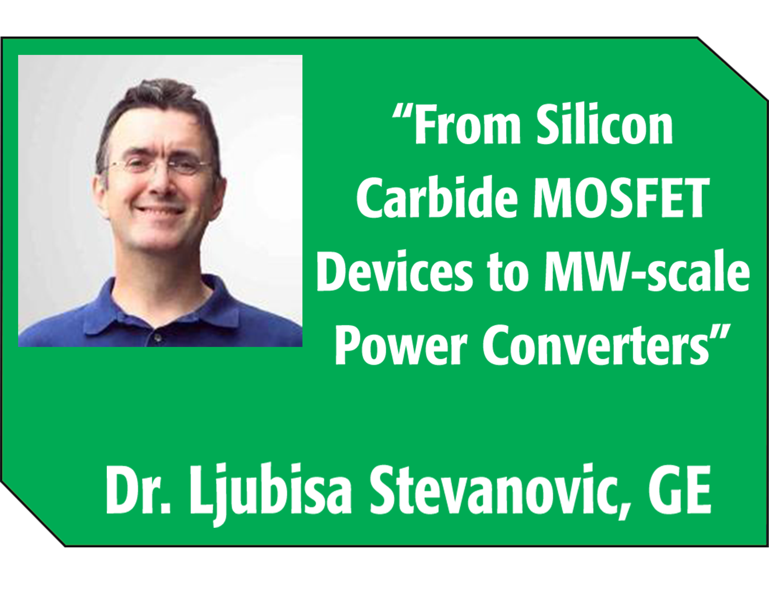
Dr. Ljubisa Stevanovic, GE Global Research

“From Silicon Carbide MOSFET Device to MW-scale
Power Converters”

Reamer Auditorium
3:35 – 4:10 pm Prof. Mona Hella, Rensselaer Polytechnic Institute
“TeraWaves: New Opportunities for Silicon Integration”
Reamer Auditorium
4:15 – 4:30 pm

Appreciation and Closing Remarks

    Prof. Luke Dosiek, Union College

Reamer Auditorium